In order to optimize your browsing experience we uses cookies. You agree to the usage of cookies when you browsing this site.
For more information regarding cookies and the processing of your personal data please read our Privacy Policy.

MARKET
Accelerate Customers Innovation
Interested in our service?
Contact Us Now!
Contact Us Now!

FULL STACK ARTIFICIAL INTELLIGENCE DEVELOPMENT FOR EDGE DEVICES USING GOAI (WHITE PAPER)
The amount of responsibility given to and expected from edge devices is growing rapidly in all types of automotive, IoT, industrial, and consumer applications. Edge inference is becoming a common capability in these devices to provide localized decision making, reduced latency and cost reduction of connected nodes.
These solutions often struggle to meet the next set of customer demands on cost, power, size as well as the flexibility to adapt and integrate over time. Additionally, the heavy computational needs of neural networks often push beyond the performance of standard microcontrollers. They also struggle from meeting time to market pressure while being expected to incorporate the latest technology advancements.
Low density FPGAs can be used to address common customer constraints on cost, power and size by providing flexible and scalable solutions dependent on the network size. GOWIN FPGA’s specifically address this by providing scalable device densities from 1k to 55K LUTs in variety of wafer level, QFN, and BGA package options as small as 3.24mm2 on both low power and high performance process technologies.

To improve performance and time to market of developing edge solutions for artificial intelligence GOWIN has created a new acceleration IP and solution suite called “GoAI” targeting their FPGA devices. The GoAI solution suite integrates GOWIN’s AI acceleration IP into existing machine learning frameworks to improve performance by over 78x compared to using a Cortex-M class microcontroller alone.

Usage of Edge AI in the System
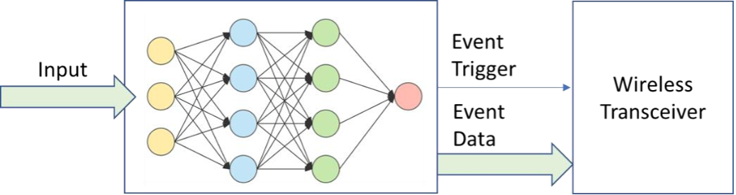
Artificial intelligence at the edge is typically used for one of two purposes in a system. The first is to perform inference with devices that have no connectivity to the internet. These systems use machine learning to detect some information about an input and utilize it to control outputs of the system that are connected to it.

The second purpose is used to perform some pre-detection before sending data to the cloud for further processing. This can be done for various reasons such as saving power by shutting off the wireless transceiver or cost by only sending data to cloud AI services when some pre-detection has occurred.
Deploying AI at the Edge
Artificial intelligence today uses the machine learning techniques centered around convolutional neural networks. These networks are essentially sets of many filters or “neurons” with coefficients or weights that are trained to identify certain key attributes of an input. These weights are calculated through a process called “training” where a set of inputs are provided, the output is known and the weights are updated to identify it.
Training a convolutional neural network often consumes a significant amount of computational power. However, since it is only used to generate the weights to infer certain attributes about the input it generally does not need to run in real time. Once a network is trained the weights can be loaded into a network to detect attributes related to the input. This inference often requires significantly less computing power than training.
While the computational power is significantly less for inferencing it often still exceeds the performance of microcontrollers. This is because microcontrollers process each computational instruction per processor clock cycle often in the sub-200Mhz range which is not enough performance to make detections of even small machine learning networks in real-time. Additionally, many use cases related to AI require specialized interfaces and buffering of data. For example, camera data often needs to be stored in RAM as a frame since filtering is performed over multiple pixels within the image at the same time.
Edge focused FPGAs address these problems easily. Parallel and pipelined computations of the network allow for real-time performance while operating the system more efficiently at 10’s of Mhz. Flexible interfacing allows the FPGA to connect to cameras, microphones, biometric sensors and other inputs easily. Configurable memories allow for buffering and retention of intermediate or layer data.
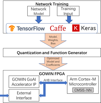
While FPGA’s provide a great avenue to make edge AI possible, a strong software stack is needed to make development and deployment easy. Modeling software for neural networks is available by several providers; Tensorflow, Caffe and Keras are common names. These networks are often natively developed using floating point computations for training and testing by the software, which causes issues when attempting to deploy a cost and performance worthy solution at the edge.
As a result, common deployment tools such as Tensorflow Lite for microcontrollers and Arm CMSIS-NN use an optimization process to truncate and quantize trained weight data from floating point to 8-bit fixed point, making the resources more practical for edge focused hardware. However, the performance is often still significant and as result an accelerator design specifically to pipeline the convolutions and accumulations of layer data is common. These accelerators can be designed in ASIC or FPGA to improve things further to real-time performance.
A System Example
To run through an entire development flow from model training to hardware design the GoAI platform was used to perform image detection on the CIFAR10 dataset. The performance of the GoAI accelerator was compared to an Arm Cortex-M microcontroller running the same network in CMISIS-NN. The CIFAR10 dataset is a common dataset of 10 classification objects used to measure various performance attributes of a machine learning system.
First, a network was trained for the system in Caffe. In this case, the network tested used three convolution layers with varying numbers of filters. After the network was trained, coefficients for weights and bias were obtained and the trained network was tested in Caffe over various inputs to ensure it behaved as expected.
After that the weight and bias coefficients were truncated and quantized using script utilities and the network was compiled to use CMISIS-NN function calls on an ARM Cortex-M1 and M3 processor. The optimized network was then deployed on the ARM Cortex-M1 processor with a camera interface and frame buffer connected to the AHB bus. The neural network took approximately 10 seconds to process one image from the camera.
Next, the GoAI accelerator was connected to the AHB bus and used to process the network. The Cortex-M1 was still used to pass image data initially to the accelerator, load weights and bias and configure the accelerator settings. The neural network took approximately 0.5 seconds to process using the GoAI accelerator with delays primarily associated with the results sent over UART.

Further analysis was performed on the Arm Cortex-M3 processor and the accelerator. The difference between using the Arm Cortex-M3 processor by standalone versus with the GoAI accelerator showed an ~78x performance improvement.
GoAI 2.0
GoAI 2.0 focuses on:
- Integration of the FPGA accelerator with TensorFlow and TensorFlow Lite
- Targeting the GOWIN GW1NSR-4C uSoC FPGA with Cortex-M3 hard processor in 6x6mm QFN package
- Software compiling and deployment SDK’s
- Flexible architecture for supporting a variety of models with large number of layers and large layer depth
The GoAI 2.0 platform uses standard TensorFlow development environments to allow training and testing of any model. The final trained model then uses TFLiteConverter or TocoConverter to parse and quantize the model into a *.tflite flatbuffers file. The flatbuffers file is then parsed using the GoAI 2.0 SDK to extract model coefficients, layer parameters and model functions.
After extracting all the necessary information from the flatbuffers file, the GoAI 2.0 SDK loads coefficients to external SPI flash memory, C code to the embedded flash of the Cortex-M3 and bitstream to the FPGA in the GW1NSR-4C device or other supported GOWIN FPGA.

The architecture of the GoAI 2.0 platform allows for as deep of layers as there is PSRAM embedded in the GW1NSR-4C and as many convolution and pooling layers as there is memory to hold layer parameters. The GW1NSR4 has 8MB of PSRAM, which is split into a 4MB input layer buffer and 4MB output buffer layer. This means that a layer input and output can be up to 4MBs in size. The ITCM embedded flash within the Cortex-M3 is 32KB, which only needs to hold the control loop and the filter parameters for each layer. The external SPI flash holds the weight and bias coefficients for each layer and can be adjusted depending on the model size required.

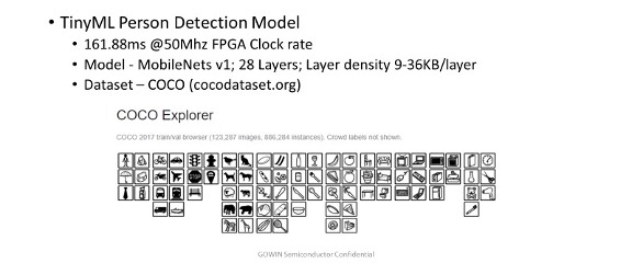
Testing of the GoAI 2.0 platform was performed using Mobilenet v1.025 and the COCO dataset. Mobilenet is a fairly large convolutional neural network with 28 layers. 162ms inference latency was achieved using GoAI 2.0 with this model.
Conclusion
Various challenges arise while attempting to efficiently perform AI at the edge within a reasonable cost, power, size and time to market budget. Artificial intelligence at the edge is becoming increasingly important for both unconnected and connected devices. Edge AI solutions require an accelerator and complete software development flow to perform real time processing and integration into common machine learning model development software. GOWIN’s GoAI accelerator and software solution stack provides an ideal solution to address both performance and market environment constraints.
Documents Download
| White Paper | White Paper of Full Stack Artificial Intelligence Development for Edge Devices using GoAI | Download |